 Hi Boox Popular Magazine 2025
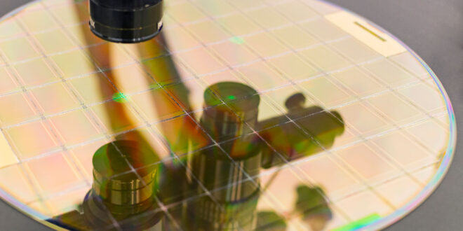
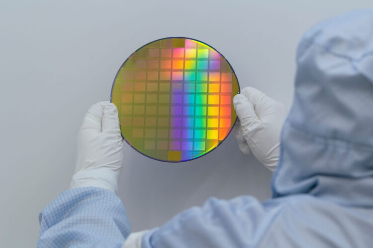
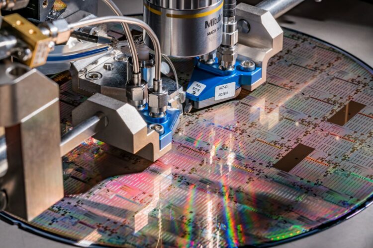
In the fast-paced and ever-evolving world of semiconductor manufacturing, precision and quality are paramount. To ensure the optimal performance and reliability of semiconductor devices, rigorous testing and evaluation are necessary. This is where test wafers come into play. Test wafers, also known as evaluation or monitor wafers, play a crucial role in the semiconductor industry by enabling the evaluation and optimization of fabrication processes.
At its core, a test wafer is a silicon or compound semiconductor substrate that replicates the structure and properties of production wafers. It serves as a surrogate for the final product and facilitates the testing and validation of various manufacturing processes. Test ones are indispensable tools used throughout different stages of semiconductor production, from research and development to process optimization, quality control, and yield enhancement.
Their Purpose
The primary purpose of test wafers is to evaluate and optimize fabrication processes in semiconductor manufacturing. By subjecting test wafers to various processing steps, semiconductor manufacturers can assess the impact of different parameters and conditions on the final device performance.
One of the key functions of test wafers is to enable the detection and rectification of issues in semiconductor manufacturing. These issues may include defects, impurities, or deviations from desired specifications.
Key Characteristics
Test wafers possess several key characteristics that make them suitable for their intended purpose. Firstly, they mimic the electrical and mechanical properties of production wafers. This ensures that the test results obtained from this kind are representative of the final device performance. Test ones typically have similar dimensions, crystal structures, and dopant concentrations as production ones.
Secondly, test wafers exhibit well-defined specifications and properties. They are precisely manufactured to meet specific requirements, such as surface roughness, flatness, and thickness uniformity. These characteristics allow engineers to evaluate the impact of different fabrication processes on the wafer and subsequently optimize the process parameters to achieve desired outcomes. For additional info please visit https://www.silybwafers.com/
Types
There are several types of test wafers, each serving a specific purpose in the semiconductor testing process. The most common types include monitor, calibration, and process control wafers.
Monitor types are used to monitor the health and performance of the fabrication process. They are typically subjected to the same processing steps as the production kind and provide valuable information about the process stability, yield, and overall quality.
Calibration ones, on the other hand, are used to calibrate the equipment used in semiconductor manufacturing. They are manufactured with precise electrical and mechanical properties, allowing engineers to ensure accurate measurements and maintain the consistency of equipment performance.
Process control type serves as a reference for process optimization. They are designed with specific structures, patterns, or layers to evaluate the performance and integrity of different process steps.
Their Role in Process Development
Test wafers play a vital role in the optimization and improvement of fabrication processes in semiconductor manufacturing. By carefully evaluating the performance of different process steps on test wafers, engineers can identify bottlenecks, eliminate inefficiencies, and enhance overall process yields.
One of the significant benefits of using test ones in process development is the ability to achieve higher yields. By analyzing test wafer data, engineers can identify process variations or issues that may lead to lower yields in production wafers. They can then fine-tune process parameters, modify equipment settings, or implement new techniques to maximize the yield and improve the overall manufacturing efficiency.
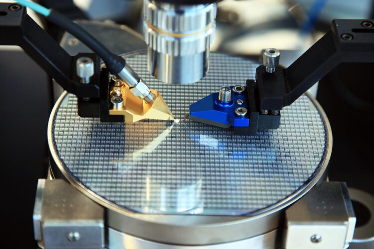
Test Wafers for Equipment Calibration
In semiconductor manufacturing, precise measurements and accurate equipment performance are crucial. Test wafers play a pivotal role in calibrating the equipment used throughout the fabrication process. Calibration ones, with their well-defined properties and specifications, provide a reference standard for equipment calibration.
By utilizing calibration wafers, semiconductor manufacturers can ensure that measurements and readings from various equipment, such as thickness gauges, ellipsometry, and profilometers, are accurate and consistent. Regular calibration using test kind minimizes measurement errors, reduces process variations, and helps maintain the overall reliability and accuracy of equipment performance.
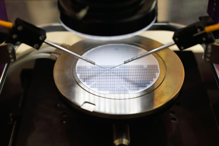
Quality Control
Quality control is of utmost importance in semiconductor manufacturing. Test wafers are instrumental in monitoring and controlling the quality of the production process. They serve as a representative sample that allows engineers to evaluate the integrity of the fabrication process and detect any deviations or defects.
They are subjected to comprehensive inspection and analysis to identify defects, impurities, or variations in critical parameters. By monitoring these characteristics, engineers can assess the effectiveness of process controls, identify potential sources of defects, and take corrective actions to improve the overall quality and reliability of the final semiconductor devices.
Test Wafers for Device Characterization
Characterizing semiconductor devices is essential for assessing their performance, reliability, and functionality. Test wafers play a crucial role in this process by providing a platform for device evaluation and analysis. By fabricating test structures or test devices on these devices, engineers can measure and analyze various electrical and physical properties.
Test wafers enable the assessment of parameters such as transistor characteristics, breakdown voltages, leakage currents, and interconnect resistance. Through comprehensive device characterization, engineers gain valuable insights into device performance, identify areas for improvement, and optimize the design and manufacturing processes to enhance the overall device quality and functionality.
Yield Enhancement
Yield improvement is a constant pursuit in semiconductor manufacturing. A test wafer plays a significant role in identifying and addressing yield-related issues. By closely analyzing test wafer data, engineers can identify the root causes of yield loss, such as process variations, defects, or equipment malfunctions.
With this information, engineers can implement targeted process improvements to minimize yield loss. They can modify process parameters, optimize equipment settings, or introduce new techniques to mitigate yield-related issues. By fine-tuning the fabrication processes based on insights gained from test wafers, semiconductor manufacturers can achieve higher product yields, reduce waste, and improve overall profitability.
Test Wafers for Research and Development
Research and development activities are vital for pushing the boundaries of semiconductor technology. Test wafers provide a platform for exploring new technologies, materials, and processes. They enable researchers and engineers to experiment with novel device structures, deposition techniques, etching processes, and material compositions.
Test wafers serve as a canvas for innovation and enable researchers to evaluate the feasibility and performance of new concepts. By utilizing test wafers in research and development, the semiconductor industry can drive advancements, discover breakthroughs, and pave the way for future technologies.
Cost Efficiency
In addition to their functional benefits, test wafers contribute to cost efficiency in semiconductor manufacturing. By utilizing test wafers throughout the fabrication process, manufacturers can optimize various aspects that lead to cost savings.
Firstly, test wafers help in process optimization, allowing manufacturers to identify and rectify process inefficiencies. By streamlining processes, reducing defects, and maximizing yields, semiconductor manufacturers can minimize waste and improve resource utilization.
Secondly, test wafers enable yield improvement. By addressing yield-related issues and optimizing process parameters, manufacturers can minimize the number of rejected or defective wafers, thereby reducing costs associated with rework or scrapped materials.